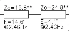
I can't understand what this E(or EL) symbol does mean. I know that Zo means impedance and I can calculate trace width according it, but what E symbol does mean?
-
Is it "electrical length" or "effective length" or something? Just a guess given that "E" is given in "degrees at a certain frequency" in the first image which makes it seem like a phase-related measurement (and maybe the EL ones in the second image are missing the degrees unit)? – natevw - AF7TB Feb 15 '23 at 18:10
-
Electrical length does not matches, because I have the physical board and it is it's schematic. – Alatriste Feb 15 '23 at 22:29
-
1Can you add a photo of this area of the physical board?, and also describe the function of the device/circuit? That context might give some clues. – Kevin Reid AG6YO Feb 16 '23 at 00:05
1 Answers
I haven't seen this notation before but it is almost certainly describing a matching section on a PCB - with two transmission lines connected together.
First is a line of 15.8 ohms impedance, 14.6 degrees long at 2.4 GHz.
On a Rogers microwave board this will be about 5-10x the board thickness wide, and about 3 mm long.
$L={1\over{\sqrt{\epsilon_r}}} {14.6\over360} {300\over2450}$ but use a real calculator because the effective $\epsilon_r$ depends a bit on the trace width.
Here's an example calculation from emcalc.com

The board must be quite thin for this to be possible at all - on a 1 mm thick board, the line would need to be 8mm wide, 1 mm long, which is a capacitor not a transmission line.
Next is a line of 25 ohms impedance, with an electrical length of just 4 degrees. I'm not sure what the point of this short line would be, but it will be 1 mm wide and 0.6 mm long.
I suspect this is a (part of a) matching section for an RF transistor. They can have impedance much lower than 50 ohms, so will benefit from a transformer.
Note that there is no wire at all between the sections, in fact they must be touching. It's just drawn like that to describe the individual parts of the line clearly.
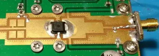
Here's a photo of an amplifier for 2.4 GHz with an SMA connector for scale, so your figures look plausible. (source: Amsat UK)

Note: 1) this is CPW not microstrip and 2) there are parallel RF-short-circuited stubs on both sides, used to supply power to the transistor.
- 11,076
- 16
- 31
-
As I said I have the physical board of that schematic, but trace width does not matches. For example: for region where Zo = 15.8, E=14.7 trace width is about 5mm and length also ~5mm. But according emcalc trace width must be ~twice less. – Alatriste Feb 16 '23 at 08:42
-
According your photo, how you did calculate trace width? according amplifier datasheet ? – Alatriste Feb 16 '23 at 08:55
-
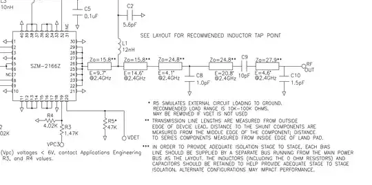
Please look at my question, I added additional full schematic image. – Alatriste Feb 16 '23 at 11:28
-
@Alatriste Which actually defines the
**and*, so you should probably have done that to begin with! Yes, that's trace length, as the footnotes say! – Marcus Müller Feb 16 '23 at 14:36 -
@MarcusMüller as I said , actual physical trace lengths does not match with footnote lengths. – Alatriste Feb 16 '23 at 14:38
-
@Alatriste how did you determine "actual physically length"? That's a phase angle, and I from the top of my head can't tell you the velocity factor of your transmission line. – Marcus Müller Feb 16 '23 at 14:44
-
@MarcusMüller please look at this picture, Actual size: I mean the trace width and length on the PCB. https://forum.amsat-dl.org/cms/index.php?attachment/5863-szm21660-jpg/ – Alatriste Feb 16 '23 at 14:48
-
@Alatriste but how do you know the phase length of the transmission line? That's not a property I can see. – Marcus Müller Feb 16 '23 at 14:49
-
@MarcusMüller Idon't know the phase length of the transmission line, how can I get it? – Alatriste Feb 16 '23 at 14:51
-
1@Alatriste you can and should calculate the line width based on your PCB Er and thickness, and whether you are using CPW or MS. If you have found an error in the reference PCB design (not shown in question) then ask about that or contact the manufacturer for errata. – tomnexus Feb 16 '23 at 15:21
-
@Alatriste But if you deviate from the reference design of the RF section, by changing the board type or thickness, I fear that a few rounds of tuning will be inevitable. Make the lines a bit too wide and cut them down carefully with a scalpel. You will alsk need a special (and expensive) probe to connect the VNA to the chip footprint. You might get away with converting to a 0.7 mm coax and soldering that. See this answer for a calibration strategy. – tomnexus Feb 16 '23 at 15:25
-
@tomnexus what if I just use 50ohm impedance tracks instead of this 15,8, 24 ohm tracks? – Alatriste Feb 16 '23 at 16:27
-
@MarcusMüller what if I just use 50ohm impedance tracks instead of this 15,8, 24 ohm tracks? – Alatriste Feb 16 '23 at 16:28
-
-
It will probably work with almost any output network (as long as you include the inductor to the power rail), but your amplifier will have maybe a quarter of its optimimum output power. Also very likely these short lines act as a filter for the 3rd and 5th harmonics (where they are closer to 90 degrees) so your amplifier will fail regulatory compliance. Maybe that doesn't matter, or you can use an external bandpass filter from mini-circuits to clean it up. – tomnexus Feb 16 '23 at 18:06


