6

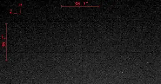
The image below is a small region of a twilight flat field. A grid of darker pixels with 728x36 cell dimensions can be seen.

enter image description here

The camera used was the SBIG STL-6303 according to the FIT headers, which uses a Kodak KAF-6303E CCD according to the online data sheet.

The CCD dimensions, these cell dimensions, and all the binning options are all perfectly divisible, so I'm assuming this artifact is due to the structure of the CCD.

I plotted the mean pixel value of each row to make sure this wasn't an artifact from the image viewing software. The plot clearly shows a drop every 36 pixels.

So, I'm hoping for some confirmation: is this decreased sensitivity due to the structure of the CCD?

If so, what about the CCD structure actually causes this?
Nilay Ghosh
  • 4,452
  • 1
  • 16
  • 45
user181339
  • 270
  • 1
  • 5

2 Answers2

6

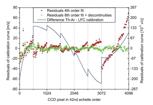
Yes, it's some sort of CCD structure originated from the manufacturing process. CCD chips with large area were produced by chunks of several hundred pixels. see http://heasarc.gsfc.nasa.gov/Images/astroe/about/xis_config.gif

And sometimes position offsets between these chunks can be detected.

CCD pixel blocks

from Wilken et al., 2010, MNRAS, 405, L16

Asterion
  • 126
  • 1
4

This looks like readout noise to me. Such noise is a consequence of the electric machinery used to convert the individual pixel detections into a digital picture, and really is an unavoidable part of CCD technology.

Take a look at this page if you want to know more about the technical details.

Michael B.
  • 1,033
  • 7
  • 8
  • There's definitely a lot of read noise, but read noise would not cause a fixed pattern (horizontal and vertical lines) like the one in the image. I should have adjusted the contrast some more - the pattern is hard to see on some monitors. – user181339 Oct 02 '14 at 15:00